


Overview:
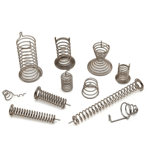
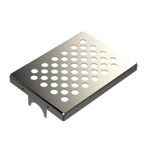
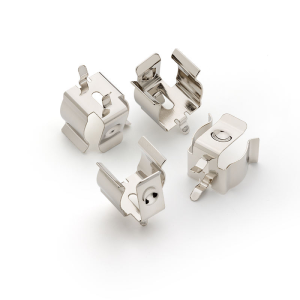
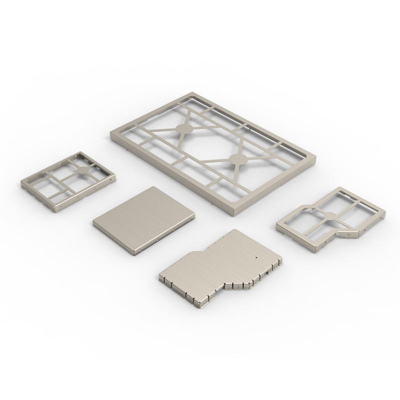
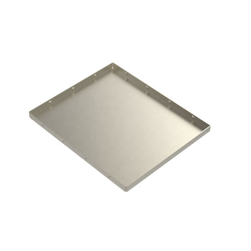
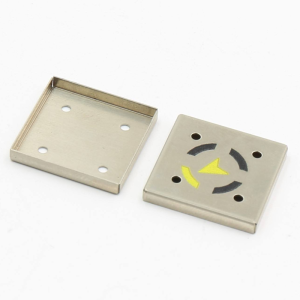
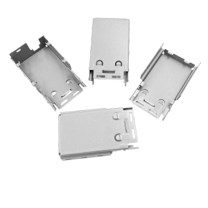
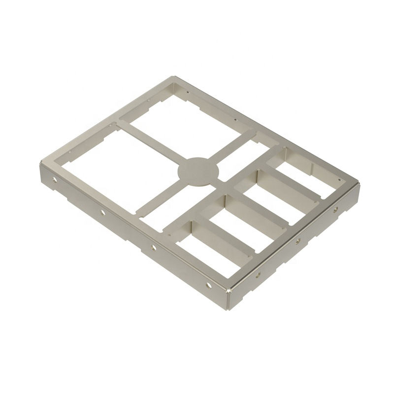
Our custom metal-stamped EMI shields are engineered to provide reliable electromagnetic interference (EMI) attenuation, mechanical protection, and precise fit for PCB assemblies. Manufactured from high-quality aluminum alloys and finished with controlled nickel plating, these shields offer lightweight, corrosion-resistant properties, with excellent conductivity at mating interfaces. We offer progressive die stamping, secondary forming, and finishing under an ISO/IATF quality system, along with full OEM services that include DFM (Design for Manufacturability), rapid tooling, mass production, and custom packaging.
Key Specifications:
| Attribute | Typical Specification |
|---|---|
| Base Material | Aluminum alloys (5052, 6061); also available: stainless steel, copper alloys |
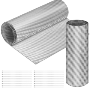
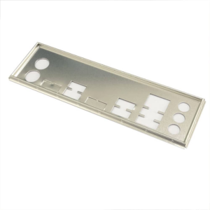
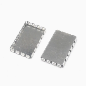
| Shield Type | Can: cover, clip-on can, enclosure, frame, connector hood |
| Material Thickness | 0.10 – 1.50 mm (customizable) |
| Dimensional Tolerance | ±0.02 mm (critical features) / ±0.05 mm (general) |
| Surface Finish | Nickel plating (electroless or electroplated) — matte/bright finish |
| Nickel Plating Thickness | 1 – 8 µm (customizable per spec) |
| Shielding Effectiveness | Typical >40–80 dB (frequency dependent, test per customer spec) |
| Forming Methods | Progressive stamping, single-hit stamping, bending, flanging |
| Secondary Processes | Laser trimming/piercing, riveting, soldering, spot welding, hemming |
| Production Capacity | Progressive stamping lines; high-volume automation available |
| Sample Lead Time | 7–14 business days (prototypes) |
| Mass Production Lead Time | 20–30 business days (after tooling approval) |
| Certification & Compliance | ISO 9001, IATF 16949 available; RoHS & REACH compliant |
| Packaging | Bulk, tray, ESD safe packaging, custom labeling |
Manufacturing Process:
- DFM & Tooling: Engineering review, 3D die design, and simulation (DFM) to optimize material use and springback.
- Blanking / Progressive Stamping: High-speed stamping on progressive dies using 25–300 ton presses to form complex geometries in multi-station operations.
- Secondary Forming: Precision bending, hemming, flanging, and crimping to achieve exact mating features on the PCB.
- Trimming & Piercing: Laser cutting or secondary punching for tight-tolerance holes and slots where required.
- Surface Preparation & Plating: Degreasing, desmut, passivation, and controlled nickel plating to specified thickness and adhesion standards.
- Assembly & Joining: Optional soldering, clinching, rivet insertion, or ultrasonic welding for multi-piece assemblies.
- Cleaning & Packaging: Ultrasonic cleaning and ESD-safe packaging; custom kits and kits with foam supports available.
Surface Treatment & Plating Options:
- Electroless Nickel (EN) Plating: Provides uniform coverage, ideal for complex geometries.
- Electro Nickel Plating: High throughput with controllable thickness and finish.
- Tin or Silver Flash: Available on request for improved solderability or conductivity.
- Passivation / Chromate Conversion: Enhances corrosion resistance prior to plating.
- Powder Coat or Anodizing: For non-conductive cosmetic finishes (not used where conductivity is required).
Quality Assurance:
All shields are manufactured under an ISO 9001 / IATF-capable quality system with full incoming material traceability. Typical QA protocols include CMM dimensional verification, surface roughness measurement, XRF/plating thickness checks, microscopic adhesion tests, salt-spray corrosion testing, and electrical continuity/contact resistance tests at mating interfaces. Shielding performance is validated in EMI test chambers per customer frequency ranges (dB attenuation reports supplied). 100% visual inspection and batch traceability are provided; FAI, PPAP, and SPC reports available on demand.
Why Choose Our EMI Shields:
- High shielding effectiveness with engineered contact features for low insertion loss
- Tight stamping tolerances and consistent repeatability for automated PCB assembly
- Flexible materials & finish options (aluminum + nickel plating standard)
- Full OEM service: DFM, rapid tooling, pilot runs, and scalable mass production
If you have PCB drawings or a shielding requirement (target dB, frequency band, mating interface), send us your Gerber or STEP files — we’ll provide a DFM review, shielding recommendations, and a fast prototype quote specific to your application.
Factory Capabilities:
Our facility is equipped with 25 high-performance punch presses, ranging from 25 to 300 tons, for both progressive and single-hit stamping. We utilize precision wire EDM and CNC grinding for die fabrication and secondary tooling, ensuring exacting tolerances and quality. Laser trimming and laser cutting technologies are employed to create fine features and prototypes, while our electroplating and metal finishing lines provide nickel, tin, silver, and passivation coatings to meet specific customer requirements. Additionally, our ultrasonic cleaning, automated assembly, and ESD-safe packaging lines guarantee that each product is handled with the utmost care, ensuring optimal performance and protection during transport.
Reviews
There are no reviews yet.